
Advances in computing and energy sciences lie at the core of mankind’s progress towards a sustainable world in the 21st century and beyond. Considering the current state-of-the-art, it is imperative that the key scientific breakthroughs will arise from understanding of charge and energy dynamics at the atomic and molecular length scales. The past three decades have seen tremendous progress in the exploration of nanometer scale materials and their fundamentally unique properties. The challenges of coming decades will involve precise control of their properties and functions when integrated into devices. Our lab focuses on these challenges of integration, assembly, and characterization of atomic scale materials into electronic and photonic devices for applications ranging from computing switches to sensors to renewable energy devices such as photovoltaics and light-emitting devices. The group focuses on four major themes described below:
Nanoelectronics:
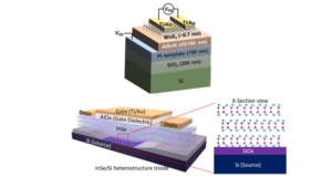
Over the past two decades, more and more 2D materials have been isolated from their bulk and studied because of their highly desirable electronic properties. Cornerstone 2D materials can be found for each band gap type. For example, MoS2, WSe2, WS2 and InSe have semiconductor properties while graphene, MoTe2, and WTe2 have metallic property, and hBN is insulator. Depending on their distinct properties, 2D materials have been widely applied to many nanoelectronics. Our lab’s research focuses on demonstrating high-performance logic devices, non-volatile memory devices, tunneling devices, neuromorphic devices etc. using various 2D materials. In addition, our group performs pioneering research on 2D/3D heterostructures. Because of the dangling bond-free nature of 2D materials, they can be stacked on 3D materials without lattice mismatch restriction, and thus it provides unprecedented chances of forming 2D/3D heterostructures.
Nanophotonics & Optoelectronics:
The effects of quantum confinement endow 2D materials with ideal properties for a multitude of technologies such as highly-efficient photovoltaics and LEDs, extremely fast beam steering, and low-threshold lasing among others. Our lab’s research focuses on confining light into deep subwavelength thicknesses to maximize light-matter interactions. In doing so, 2D materials enable us to control light in ways that were not possible in the current generation of photonic and opto-electronics that are typically based on silicon and III-V semiconductors.
Functional Imaging:
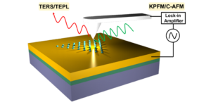
All physical phenomena of nanomaterials occur on the sub-wavelength scale i.e. charge & energy transfer, photoluminescence, and light-matter interactions. Therefore, direct optical imaging of nanoscale objects is important to understand the optoelectronic properties of nanomaterials. Taking advantage of tip-enhanced optical micro-spectroscopy, the research in our lab is grounded upon directly measuring and analyzing concurrent optical and electrical maps of different types of nanomaterials (0D quantum dot, 1D CNTs, and 2D semiconductors) and their mixed-dimensional interfaces to give an overall assessment of the interface characteristics. By doing so, we can evaluate semiconductor-metal contacts, quantum emitters, and strong light-matter interactions (exciton-plasmon-polariton coupling).
Growth and Synthesis:
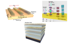
Silicon has dominated the electronic and optics industries since the mid-20th century not necessarily due its electronic and optical properties, but instead because of the ability to produce ultra-high quality, large area wafers that are easy to work with. An intense push into the research of 2D materials in the past 20 years have shown that atomically thin materials can outperform silicon on the lab bench, but it is still difficult to produce high-quality, 2D materials on a large scale. Our group uses the tools at the Singh Center for Nanotechnology to produce multiple different atomically thin materials. Our focus is on using metal-organic chemical vapor deposition (MOCVD) to grow large area samples.